What’s New in Altium Designer
When accessing the Constraint Manager from the PCB editor and defining constraints on the Physical and Electrical views, it is now possible to transfer those constraints to the Schematic through the Engineering Change Order (ECO) process. This enhancement ensures design consistency by reducing errors and saving time in the constraint definition process.
RECOMMENDED CONTENT
To see an overview about the Constraint Manager, visit the feature page.
To see the Constraint Manager in action, check out our recent webinar Empowering Faster Electronics Development with Altium Designer 24.
Check out our recent OnTrack Podcast video on the Constraint Manager, Deep Diving Into Altium Designer's New Constraint Manager.
Visit the Constraint Manager documentation page to learn more.
Altium Designer has added support for multi-colored wires, with the ability to define primary, secondary, tertiary, and border colors as part of a wire's parameters to help expand the functional identification capability of wires in your design.
RECOMMENDED CONTENT
To see an overview about the Harness Design tool, visit the feature page.
Check out our recent webinar on Harness Design, Future-Proof your Wire Harnesses with Altium Designer.
Visit the Harness Design documentation page to learn more.
You now have the ability to manually map components in target blocks where multiple components have been detected by the PCB Layout Replication Tool as having similar connections. This allows you to manually choose between available components that are able to replace each other, without violating circuit connectivity.
RECOMMENDED CONTENT
To see the PCB Layout Replication in action, check out our demonstration video.
Visit the PCB Layout Replication documentation page to learn more.
Altium Designer's Constraint Manager, with significant enhancements in design control, is now more flexible and intuitive. Efficiency in design organization is improved with the capability of adding nets to an existing class. Custom topologies are defined more insightfully with structured xSignals, and we’ve also added line numbers on tabs/grids to enhance clarity and navigation. Lastly, you can now choose between the Constraint Manager and the older Design Rules system when creating a new project to adapt to your preferred workflow.
Altium Designer's latest PCB CoDesign enhancements offer a more efficient and streamlined collaboration process. You can now precisely compare and apply changes to unions for targeted modifications. Also, the ‘Show on PCB’ option simplifies highlighting changes in specific categories for better visualization. These improvements aim to boost efficiency and provide a more organized and seamless collaborative design experience.
Altium Designer's Multi-board Draftsman tool integrates manufacturing drawings into Multi-board design projects. The multi-board view displays combined graphics of PCB outlines and 3D models with various viewing options. Enjoy standard Draftsman features like annotation, dimensioning, and BOM, and say goodbye to managing different documentation sets or relying solely on MCAD software. Draftsman for Multi-board offers a clear visual representation of board connections in larger systems, ensuring design integrity and consistency.
Altium Designer introduces the Simulation Stress Analysis tool, which enhances the design process by incorporating stress analysis within transient analysis. This tool calculates and checks component operating conditions against defined limits, simplifies stress model creation, and allows for reliability derating. With a comprehensive stress chart in the simulation viewer, it provides precision and control for informed decisions on component reliability and performance.
Altium Designer's Constraint Manager, available for pro and enterprise subscriptions, simplifies meeting complex standards and PCB design requirements. This tool allows easy browsing, creation, modification, and reuse of verified constraint sets through a tabular, object-based user interface. Enhancing clarity and comprehension, it seamlessly integrates rules between schematics and PCB layout, streamlining the design process with a consistent format for rule addition in both areas.
Altium Designer's PCB CoDesign simplifies collaboration, ensuring design integrity for engineering teams. With pro and enterprise subscriptions, this tool streamlines cooperation within your workspace, eliminating manual change tracking. Visualize alterations, compare layouts, and merge updates effortlessly in a unified environment. Say goodbye to cumbersome revision histories and embrace a more efficient PCB design approach with PCB CoDesign.
Altium Designer introduces the groundbreaking 3D Mechatronic Integrated Device design tool, simplifying the integration of non-planar electronic designs. It seamlessly aligns with existing components, synchronizes with schematic documents, and eliminates the need for time-consuming M-CAD hacks. This tool meets electrical specifications while enabling aesthetically pleasing designs. With pro or enterprise subscriptions, it facilitates easy adoption in your product development workflow.
Altium Designer's enhanced Power Analyzer by Keysight Tool addresses power network analysis challenges efficiently. With new support for assigning currents to multiple nets on the same component across different series elements. This enhancement ensures a seamless and efficient power analysis experience, allowing you to maximize benefits from your design in Altium Designer.
Automatic Length Tuning introduces automatic length and delay tuning functionality in 2D mode, accessed conveniently from the main Route menu. This feature reduces the manual effort typically associated with length and delay tuning, expediting your design process.
For enterprise and pro subscriptions, the new Constraint Manager offers a table-based interface, accessible from both Schematic and PCB, allowing you to define constraints more collaboratively. Engineers and stakeholders can collectively set design constraints with ease.
The new PCB Layout Replication tool gives you the ability to quickly replicate the layout for repetitive blocks of circuitry in a flat PCB design. This avoids the need for manual routines, snippets, reuse blocks, or converting into a multi-channel design.
The custom paste and solder mask feature is now automatically enabled by default, allowing you to personalize pad shapes directly without the need for workarounds. This simplification improves manufacturing efficiency, project clarity, and provides a more user-friendly interface.
We've added a new "Retrace Parameters" feature to the Gloss and Retrace panel, offering enhanced flexibility for retracing single-ended traces at any angle using the Rounded hugging style. You can also set rule-based width modes or input custom values to ensure compliance with design rules. Furthermore, you have the option to "Preserve Route Path," allowing you to maintain precise trace geometry during retracing, providing greater control and design accuracy.
Altium Designer's "Where Used" component panel streamlines component management in your PCB designs. It offers a comprehensive list of where each component is used, making conflict resolution and maintaining design accuracy a breeze. The latest enhancement features a redesigned panel and integration of Reuse Blocks from the connected Workspace's library, with tabs displayed only when relevant to reduce clutter.
For Pro and Enterprise subscriptions, PCB CoDesign in Altium Designer revolutionizes collaborative design by enabling multiple team members to work simultaneously on a project, ensuring streamlined development, efficient testing, and faster iteration to meet project deadlines. This feature includes Git-like version control, allowing collaborators to access the same project concurrently, commit changes to a master branch, and use Commenting and Tasks features to allocate work on the board. Notifications alert team members of commits, and the Compare and Merge panel displays differences in design, offering color-coded feedback. When conflicts arise, such as overlapping changes by multiple designers, you can confidently decide to keep local changes or accept remote changes from the latest commit, ensuring a smooth collaborative design process.
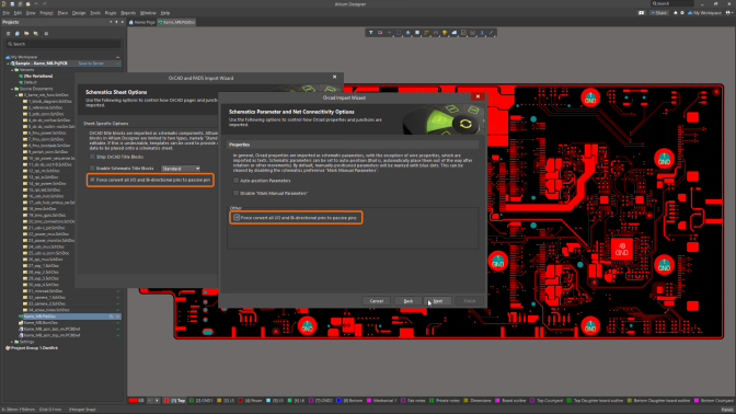
There are key improvements and fixes in relation to the import of OrCAD and Allegro design files into Altium Designer. This includes support for customized port connectors, accurate title block parameter handling, component fill coloring preservation, and precise design file imports, ensuring your design process is seamless.
For enterprise, when connected to an Enterprise Server Workspace and a design project is stored in a SVN repository managed through the Workspace's Version Control Service, you can now migrate this project from the SVN repository to the Workspace's built-in Git repository.
When it comes to license management, the search field and related sorting control will now appear only when more than seven licenses are in the listing to avoid redundancy. Also, license type labels have been added to help quickly distinguish differences between licenses in the listing.
For Harness Design, the zoom level now sets the size of the model view's green box automatically. No need for manual adjustments. We've also added quick keyboard shortcuts for adding wires and placing bundles to streamline your workflow. Plus, you can easily validate your active harness project with the new validate button.
There is a new functionality of the ‘Copy Room Formats’ feature with the addition of an option to control whether or not the rotation of the chosen source room is copied to the desired destination room, avoiding the need for manual rotation corrections.
You can now include a wider range of manufacturing and assembly parameters, such as layer counts, board dimensions, and object quantities directly into your fabrication and assembly notes. These additions are conveniently auto-calculated directly from the PCB, ensuring that your notes align with any design updates.
Altium has completed the custom pad stack feature, which includes the ability to freely customize pad, thermal relief, and most recently, paste and solder mask shapes. You now have the ability to independently control paste and solder mask shapes and can adapt to non-standard component footprints.
Altium has added the ability to manage part choices that are associated with each component in your design. The excluded part choice will still be in the project, however it will not appear in the generated BOM, nor will it be used in price calculations or as part of BOM checks
The new Mixed-Simulation Data Viewer introduces higher waveform accuracy and measurement precision. This extended precision significantly reduces the likelihood of round-off errors, ensuring more accurate results when viewing simulation waveforms to improve the overall reliability of the simulation process.
Altium has expanded support for additional multi-board features, which allows you to navigate to your wiring diagrams seamlessly from your multi-board schematic. You are now able to cross-probe directly from the corresponding harness object on the multi-board schematic to the Wiring Diagram of that harness design, minimizing the risk of mismatch and giving you more control over your multi-board design.
The latest release simplifies the management of the silkscreen preparation process, offering the ability to effortlessly move or clip silkscreen objects at specific distances from exposed copper or solder mask openings. This eliminates the need for manual silkscreen work while creating footprints and PCB manufacturing preparation.
Altium's latest release adds simulation capabilities by providing expanded support for additional components. You are now able to add your digital file stimulus device (FSTIM) model primitives from PSpice for simulation in Altium to achieve high accuracy and efficiency in generating transient signals. This addition aligns with Altium's ongoing commitment to have a best-in-class SPICE simulator fully integrated within the Altium Designer environment.
This release introduces new tools for precise harness cable design, helping to reduce errors during assembly. You can now define the size of the harness covering relative to the enclosed bundle and choose between solid-style and patterned fills. Additionally, isometric views in the Layout Drawing give assemblers an additional viewpoint to enhance the presentation of harness components, enabling comprehensive communication of design intent and minimizing assembly errors.
The PCB section view provides precise insight into the layout and structure of your designs, like never before. when working with dense and complex PCBs the section view reveals the details within a PCB that are typically not visible. With full control over plane placement and color you can easily see all components, even smaller SMD components hiding under larger components or mechanical parts.
As a continuation of our custom pad shape capabilities, it is now possible to add, remove, and edit, thermal relief spikes to anywhere on a pad, regardless of shape. This helps with soldering and avoids possible manufacturing problems like tombstoning.
The interactive probes feature is like using an oscilloscope right within Altium Designer. When this feature is enabled, any changes to probe placement, color, or other settings, are immediately reflected in the simulation results document.
We’ve now added support for voltage and current controlled sources, functional sources and variable passive components for voltage, power and current output variables in the AC analysis. Great for audio projects, communication designs, and other design types. Plus we’ve added support for multi-bit ADC and ROM PSPICE digital model primitives as well as their timing models.
Live traces actively follow your cursor, showing you the way to your final wire destination. Allowing you to move more efficiently in the wiring diagram. Wiring diagram objects are now synced with the documents snap grid, bringing a new level of uniformity to the diagram.
In the Layout Drawing, it is now possible to show the Physical (3D) model for a connector as a wireframe view and also, for a connection point, display the Physical (3D) model of one of its associated parts.
For this release we have added support for workspace defined project parameters, bulk creation and edits of components, and enhanced side-by-side component revision comparison.
This release of Altium Designer we’ve added support for more programmable logic array PSPICE digital primitives as well as support for digital models that use global nodes ($D_HI, $D_LO, $D_X), and variable passives.
The wiring diagram and layout drawing for harness projects has been given several new features to boost usability. We’ve added additional crimping capabilities, scaling options for documentation, visual connection lines for components and more.
The Gerber Setup dialog now includes a Layer Classes section in its Layers to plot list. Using the checkbox for layer classes, you can quickly enable plotting for all the layers that belong to a specific layer class.
This release of Altium Designer supports even more PSPICE digital model primitives. We’ve added support for the PINDLY, and CONSTRAINT Pspice digital behavioral model primitives as well as support for the DIGRRGEFAULT option.
In this release of Altium Designer we’ve added several new features to boost the usability of the harness wiring diagram and layout drawing. Including additional features for crimping, splices, and efficiency
To better convey a message to other project stakeholders, you now have the capability to copy and paste pictures into your comments. Also, exporting a project history report can now be easily done through the Reports menu.
This release has added several improvements for both the harness wiring diagram and the Harness layout drawing. Some new capabilities include: parameters for twist and shield objects, crimping, additional 3D views, multiple connections from a single point and more…
New PCB features allow you to load a stored view configuration file from the View Configuration Panel. Also, it is now possible to change the name for the Gerber Board Profile layer when using the new, unified Gerber/Gerber X2 dialog.
Shape your pads the way you need in a matter of clicks. Extending the versatility of pad shapes, you can now customize the rounding of selected corners of pads that use either the Rounded Rectangle shape or the new Chamfered Rectangle shape.
Efficiency, simplicity and convenience are all delivered with the new UI for Gerber setup. Everything you need to prepare for Gerber generation is now at your fingertips in an intuitive setting.
Expanding the functionality available to you in the simulation arena, this release adds further support for PSPICE digital gates, timing and I/O models. Support for variants is also now available.
Altium Designer can also be purchased as a perpetual license. Single seat, unlimited term licenses of any product types. The perpetual license comes with one year of subscription.
Contact us for a 15-day full featured evaluation license with no technical limitations. We'll send you an email with access to the trial so be sure to check that your address is correct.