What’s New in Altium Designer 2023
What’s New in Altium Designer 2023
Explore new features, enhancements, and important changes introduced in the latest version of Altium Designer, or see what we’re working on now for upcoming releases.
Altium Designer 23
Tackle Any Design Complexity With the Constraint Manager
Tackle Any Design Complexity With the Constraint Manager
Speed Up Your Workflow With the Power of PCB Layout Replication
Speed Up Your Workflow With the Power of PCB Layout Replication
The new PCB Layout Replication tool gives you the ability to quickly replicate the layout for repetitive blocks of circuitry in a flat PCB design. This avoids the need for manual routines, snippets, reuse blocks, or converting into a multi-channel design.
Minimize Manual Effort With Automatic Length Tuning
Minimize Manual Effort With Automatic Length Tuning
Automatic Length Tuning introduces automatic length and delay tuning functionality in 2D mode, accessed conveniently from the main Route menu. This feature reduces the manual effort typically associated with length and delay tuning, expediting your design process.
Easily Edit Paste and Solder Mask Shapes
Easily Edit Paste and Solder Mask Shapes
Retrace Single-Ended Traces at any Angle
Retrace Single-Ended Traces at any Angle
We’ve added a new “Retrace Parameters” feature to the Gloss and Retrace panel, offering enhanced flexibility for retracing single-ended traces at any angle using the Rounded hugging style. You can also set rule-based width modes or input custom values to ensure compliance with design rules. Furthermore, you have the option to “Preserve Route Path,” allowing you to maintain precise trace geometry during retracing, providing greater control and design accuracy.
Track Components in Reuse Blocks with the “Where Used” Panel
Track Components in Reuse Blocks with the “Where Used” Panel
Altium Designer’s “Where Used” component panel streamlines component management in your PCB designs. It offers a comprehensive list of where each component is used, making conflict resolution and maintaining design accuracy a breeze. The latest enhancement features a redesigned panel and integration of Reuse Blocks from the connected Workspace’s library, with tabs displayed only when relevant to reduce clutter.
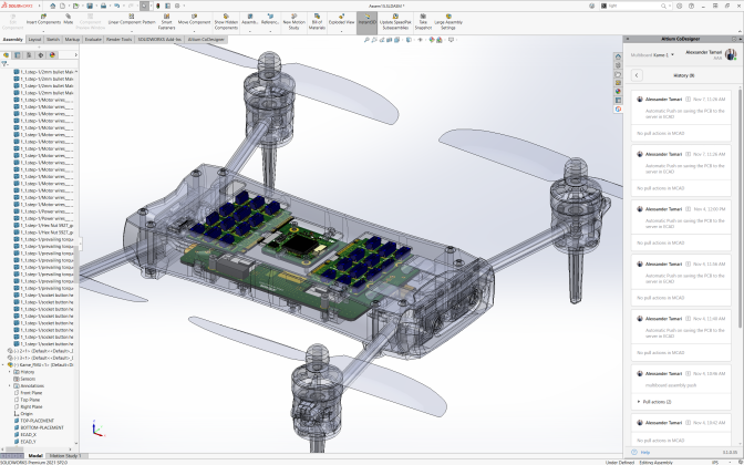
Efficient Concurrent Design with PCB CoDesign
Efficient Concurrent Design with PCB CoDesign
For Pro and Enterprise subscriptions, PCB CoDesign in Altium Designer revolutionizes collaborative design by enabling multiple team members to work simultaneously on a project, ensuring streamlined development, efficient testing, and faster iteration to meet project deadlines. This feature includes Git-like version control, allowing collaborators to access the same project concurrently, commit changes to a master branch, and use Commenting and Tasks features to allocate work on the board. Notifications alert team members of commits, and the Compare and Merge panel displays differences in design, offering color-coded feedback. When conflicts arise, such as overlapping changes by multiple designers, you can confidently decide to keep local changes or accept remote changes from the latest commit, ensuring a smooth collaborative design process.
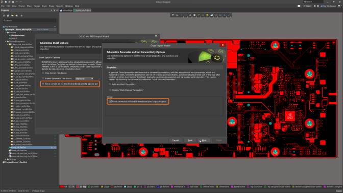
Seamlessly Import OrCAD and Allegro Design Files
Seamlessly Import OrCAD and Allegro Design Files
There are key improvements and fixes in relation to the import of OrCAD and Allegro design files into Altium Designer. This includes support for customized port connectors, accurate title block parameter handling, component fill coloring preservation, and precise design file imports, ensuring your design process is seamless.
Migrate Projects from SVN to Git in Your Enterprise Server Workspace
Migrate Projects from SVN to Git in Your Enterprise Server Workspace
For enterprise, when connected to an Enterprise Server Workspace and a design project is stored in a SVN repository managed through the Workspace’s Version Control Service, you can now migrate this project from the SVN repository to the Workspace’s built-in Git repository.
Optimize License Management with Enhanced Navigation and Labels
Optimize License Management with Enhanced Navigation and Labels
When it comes to license management, the search field and related sorting control will now appear only when more than seven licenses are in the listing to avoid redundancy. Also, license type labels have been added to help quickly distinguish differences between licenses in the listing.
Unlock More Efficient Harness Design Features and Easily Validate Projects
Unlock More Efficient Harness Design Features and Easily Validate Projects
Simply Copy Room Format with Rotation
Simply Copy Room Format with Rotation
There is a new functionality of the ‘Copy Room Formats’ feature with the addition of an option to control whether or not the rotation of the chosen source room is copied to the desired destination room, avoiding the need for manual rotation corrections.
Add New Special Strings for Fabrication and Assembly Notes
Add New Special Strings for Fabrication and Assembly Notes
You can now include a wider range of manufacturing and assembly parameters, such as layer counts, board dimensions, and object quantities directly into your fabrication and assembly notes. These additions are conveniently auto-calculated directly from the PCB, ensuring that your notes align with any design updates.
Freely Customize Paste Mask and Solder Mask
Freely Customize Paste Mask and Solder Mask
Altium has completed the custom pad stack feature, which includes the ability to freely customize pad, thermal relief, and most recently, paste and solder mask shapes. You now have the ability to independently control paste and solder mask shapes and can adapt to non-standard component footprints.
Conveniently Manage Part Choices for Each Component in Your Design
Conveniently Manage Part Choices for Each Component in Your Design
Altium has added the ability to manage part choices that are associated with each component in your design. The excluded part choice will still be in the project, however it will not appear in the generated BOM, nor will it be used in price calculations or as part of BOM checks
Precisely Measure your Results with the New Simulation Data Viewer
Precisely Measure your Results with the New Simulation Data Viewer
The new Mixed-Simulation Data Viewer introduces higher waveform accuracy and measurement precision. This extended precision significantly reduces the likelihood of round-off errors, ensuring more accurate results when viewing simulation waveforms to improve the overall reliability of the simulation process.
Easily Keep Track of your Harness Wiring Diagrams
Easily Keep Track of your Harness Wiring Diagrams
Altium has expanded support for additional multi-board features, which allows you to navigate to your wiring diagrams seamlessly from your multi-board schematic. You are now able to cross-probe directly from the corresponding harness object on the multi-board schematic to the Wiring Diagram of that harness design, minimizing the risk of mismatch and giving you more control over your multi-board design.
Precisely Position Silkscreen for Footprint Creation and PCB Manufacturing Preparation
Precisely Position Silkscreen for Footprint Creation and PCB Manufacturing Preparation
The latest release simplifies the management of the silkscreen preparation process, offering the ability to effortlessly move or clip silkscreen objects at specific distances from exposed copper or solder mask openings. This eliminates the need for manual silkscreen work while creating footprints and PCB manufacturing preparation.
Utilize the FSTIM Stimulus Model During Simulation
Utilize the FSTIM Stimulus Model During Simulation
Altium’s latest release adds simulation capabilities by providing expanded support for additional components. You are now able to add your digital file stimulus device (FSTIM) model primitives from PSpice for simulation in Altium to achieve high accuracy and efficiency in generating transient signals. This addition aligns with Altium’s ongoing commitment to have a best-in-class SPICE simulator fully integrated within the Altium Designer environment.
Create Your Harness Cable Assembly Drawing Even More Precisely
Create Your Harness Cable Assembly Drawing Even More Precisely
This release introduces new tools for precise harness cable design, helping to reduce errors during assembly. You can now define the size of the harness covering relative to the enclosed bundle and choose between solid-style and patterned fills. Additionally, isometric views in the Layout Drawing give assemblers an additional viewpoint to enhance the presentation of harness components, enabling comprehensive communication of design intent and minimizing assembly errors.
Import Values from Directives in the Constraint Manager
Discover the hidden parts of your board with the pcb section view
The PCB section view provides precise insight into the layout and structure of your designs, like never before. when working with dense and complex PCBs the section view reveals the details within a PCB that are typically not visible. With full control over plane placement and color you can easily see all components, even smaller SMD components hiding under larger components or mechanical parts.
Custom Thermal Reliefs for Pads
Custom Thermal Reliefs for Pads
As a continuation of our custom pad shape capabilities, it is now possible to add, remove, and edit, thermal relief spikes to anywhere on a pad, regardless of shape. This helps with soldering and avoids possible manufacturing problems like tombstoning.
Test Your Circuits With Real-Time Simulation Probes
Test Your Circuits With Real-Time Simulation Probes
The interactive probes feature is like using an oscilloscope right within Altium Designer. When this feature is enabled, any changes to probe placement, color, or other settings, are immediately reflected in the simulation results document.
Circuit Simulation support for Output Values in AC Analysis for Controlled Sources and Variable Passives
Circuit Simulation support for Output Values in AC Analysis for Controlled Sources and Variable Passives
We’ve now added support for voltage and current controlled sources, functional sources and variable passive components for voltage, power and current output variables in the AC analysis. Great for audio projects, communication designs, and other design types. Plus we’ve added support for multi-bit ADC and ROM PSPICE digital model primitives as well as their timing models.
Live Traces & Fixed Aspect Ratios for Harness Wiring Diagram Objects
Live Traces & Fixed Aspect Ratios for Harness Wiring Diagram Objects
Live traces actively follow your cursor, showing you the way to your final wire destination. Allowing you to move more efficiently in the wiring diagram. Wiring diagram objects are now synced with the documents snap grid, bringing a new level of uniformity to the diagram.
New in Harness Design: 3D wireframe View And Ability to Add Models to Connection Points
New in Harness Design: 3D wireframe View And Ability to Add Models to Connection Points
In the Layout Drawing, it is now possible to show the Physical (3D) model for a connector as a wireframe view and also, for a connection point, display the Physical (3D) model of one of its associated parts.
Support For Workspace Defined Parameters & Bulk Edits For Components
Support For Workspace Defined Parameters & Bulk Edits For Components
For this release we have added support for workspace defined project parameters, bulk creation and edits of components, and enhanced side-by-side component revision comparison.
Added Support for Variable Passives & Global Nodes
Added Support for Variable Passives & Global Nodes
This release of Altium Designer we’ve added support for more programmable logic array PSPICE digital primitives as well as support for digital models that use global nodes ($D_HI, $D_LO, $D_X), and variable passives.
Harness Design Improvements
Harness Design Improvements
The wiring diagram and layout drawing for harness projects has been given several new features to boost usability. We’ve added additional crimping capabilities, scaling options for documentation, visual connection lines for components and more.
Gerber Setup Layer Class Support
Gerber Setup Layer Class Support
The Gerber Setup dialog now includes a Layer Classes section in its Layers to plot list. Using the checkbox for layer classes, you can quickly enable plotting for all the layers that belong to a specific layer class.
Added Support for PSpice Digital models
Added Support for PSpice Digital models
This release of Altium Designer supports even more PSPICE digital model primitives. We’ve added support for the PINDLY, and CONSTRAINT Pspice digital behavioral model primitives as well as support for the DIGRRGEFAULT option.
Harness Design Improvements
Harness Design Improvements
In this release of Altium Designer we’ve added several new features to boost the usability of the harness wiring diagram and layout drawing. Including additional features for crimping, splices, and efficiency
Update to Collaboration and Reporting
Update to Collaboration and Reporting
To better convey a message to other project stakeholders, you now have the capability to copy and paste pictures into your comments. Also, exporting a project history report can now be easily done through the Reports menu.
Additional Harness Design Capabilities
Additional Harness Design Capabilities
This release has added several improvements for both the harness wiring diagram and the Harness layout drawing. Some new capabilities include: parameters for twist and shield objects, crimping, additional 3D views, multiple connections from a single point and more…
New PCB Capabilities for Gerber and View Configuration
New PCB Capabilities for Gerber and View Configuration
New PCB features allow you to load a stored view configuration file from the View Configuration Panel. Also, it is now possible to change the name for the Gerber Board Profile layer when using the new, unified Gerber/Gerber X2 dialog.
New Extension For Power Integrity Analysis
New Extension For Power Integrity Analysis
Quickly assess the integrity of your power distribution network without the need for any specialized training with Power Analyzer by Keysight.
Multi-board support In MCAD CoDesigner
Multi-board support In MCAD CoDesigner
You are now able to transfer and sync your muli-board designs with your mechanical team using the MCAD CoDesigner.
New Harness Design Capabilities
New Harness Design Capabilities
Harness Design functionality allows you to create a full wiring harness design, from the individual pin-to-pin connections right through to manufacturing documentation.
Want to stay UpToDate?
Join our learning community to stay informed about our upcoming training sessions, online lessons, and special offers. Enhance your skills with our expert-led courses and get the latest updates directly from our local branch.
Sign up for our email newsletter to keep learning and growing with us!