


Schematic Capture Improvement
Added Ability to Define Pin's Vertical Margin
You now define a custom vertical margin for a pin’s designator and name. This gives you full control over horizontal (X) and vertical (Y) margins. Margins can be defined globally on the Schematic – General page of the Preferences dialog in the Pin Settings region in the Designator and Margin (X/Y) fields. To define margins locally, use the Margin (X/Y) fields in the Properties panel.
Define pin vertical margins locally on the Properties panel.
The pin’s vertical margin is defined using the new Pin Designator Vertical Margin and Pin Name Vertical Margin fields in the List panels and the Find Similar Objects dialog. In addition, two new query keywords are available in the SCH Functions\Fields category – PinDesignator_CustomPosition_VerticalMargin and PinName_CustomPosition_VerticalMargin – for targeting the vertical margin of these two properties when crafting logical query expressions.
PCB Design Improvement
ODB++ Intellectual Property Protection (Open Beta)
This release brings the ability to configure ODB++ setup to protect your valuable intellectual property (IP) by restricting what is generated.
In the ODB++ Setup dialog, you have the ability to select which signal layers to export as part of the generated data. In addition, you can control whether the netlist is included and, if so, whether to neutralize it (by replacing net names with Net_[1-…]). You also can control whether to include components, with the possibility to remove component properties (parameters).
There is currently a limitation in that ODB++ data generated with no signal layers and dielectrics at all, along with export of drill-pair data, will not import into CAMtastic in a previous version of Altium Designer. It is advised to follow one of the following workarounds:
Import the generated ODB++ data into the CAMtastic editor of this latest version of Altium Designer. It can then be saved and will open correctly in the CAMtastic editor in a previous version of the software.
If you need to exclude all copper/dielectric layers from generated ODB++ data, disable export of drill pairs as well.
If exporting drill pairs, then include at least one signal layer in the exported ODB++ data.
This feature is in Open Beta and available when the ODB.IntellectualPropertyProtection option is enabled in the Advanced Settings dialog.
Folder path information will also be removed from generated report ([Design name].REP) and rule (odb\user\[Design name].RUL) files.
Wire Bonding Improvement
Wire Bonding 3D Enhancements (Open Beta)
This release brings enhanced support for bond wires in the 3D view of a board. This includes:
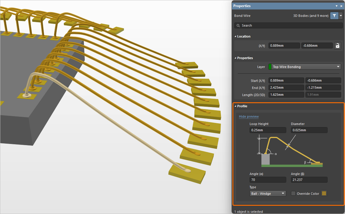
Additional editing controls for defining the shape/profile of a bond wire. You can now specify a start Angle (α) and end Angle (β).
Note that when Angle (α) is set to 90, the value of Angle (β) is defined automatically and cannot be changed.
The Die Bond Type option has been renamed Type, with a more intuitive selection that reflects the start and end of the bond wire (either Ball – Wedge or Wedge – Wedge). You also have the ability to enable and specify an Override Color for a bond wire. This facilitates being able to distinguish between different bond wire ‘tiers’ associated with different cycles of a wire bonding machine when generating a wire bonding assembly diagram.
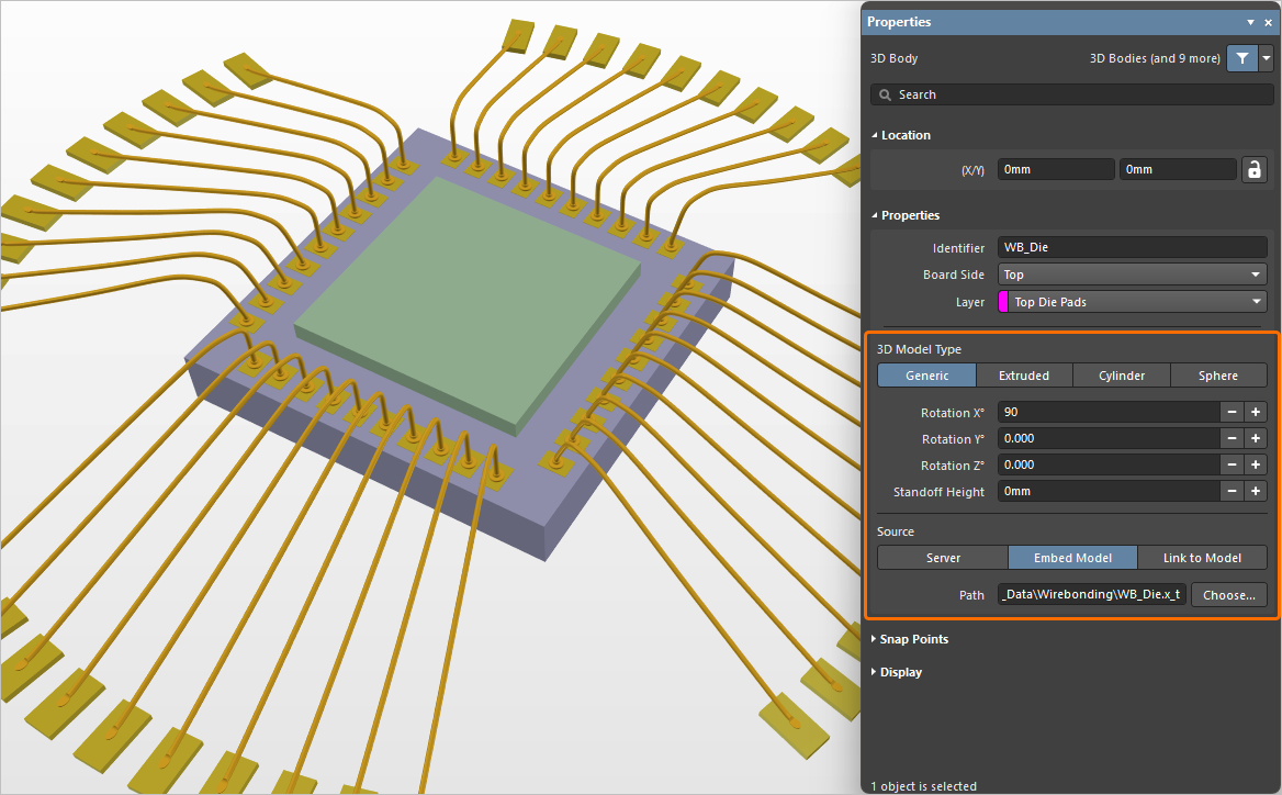
The ability to place die pads and bond wires on generic 3D bodies (STEP, SOLIDWORKS Part and Parasolid model formats, as well as extruded 3D bodies). When placed on a generic 3D body, die pads will be automatically placed at the body height under the pad center.
The inclusion of bond wire objects in Component Clearance checking, to detect clearance violations between bond wires and other (non bond wire) objects in the 3D space.
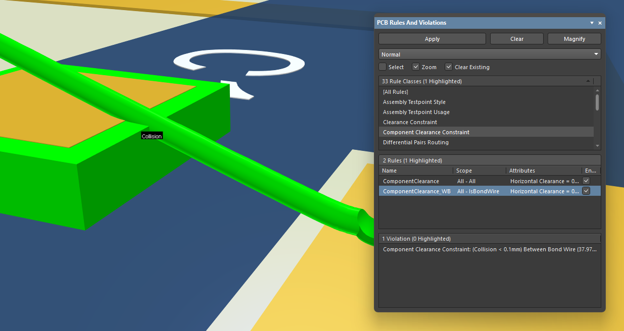
Note that bond wire to bond wire distance is detected, as before, through use of a Wire Bonding rule.
In addition, colors used for bond wires in the PCB design are now taken into account when placing a board fabrication view, board assembly view and component view into a PCB manufacturing drawing (*.PCBDwf). You can choose to use the layer color or override color (if specified for bond wires on the PCB side).
An example of Draftsman's board fabrication view with bond wires shown with their override colors. Note that the relevant Wire Bonding layer needs to be enabled on the Layer tab of the view's Properties panel.
Also, when using the enhanced support for bond wires, the following features are available:
Bond Wires is available to be added as an object to the Selection Filter, accessed from the Active Bar and the Properties panel (pre- and post-selection filtering).

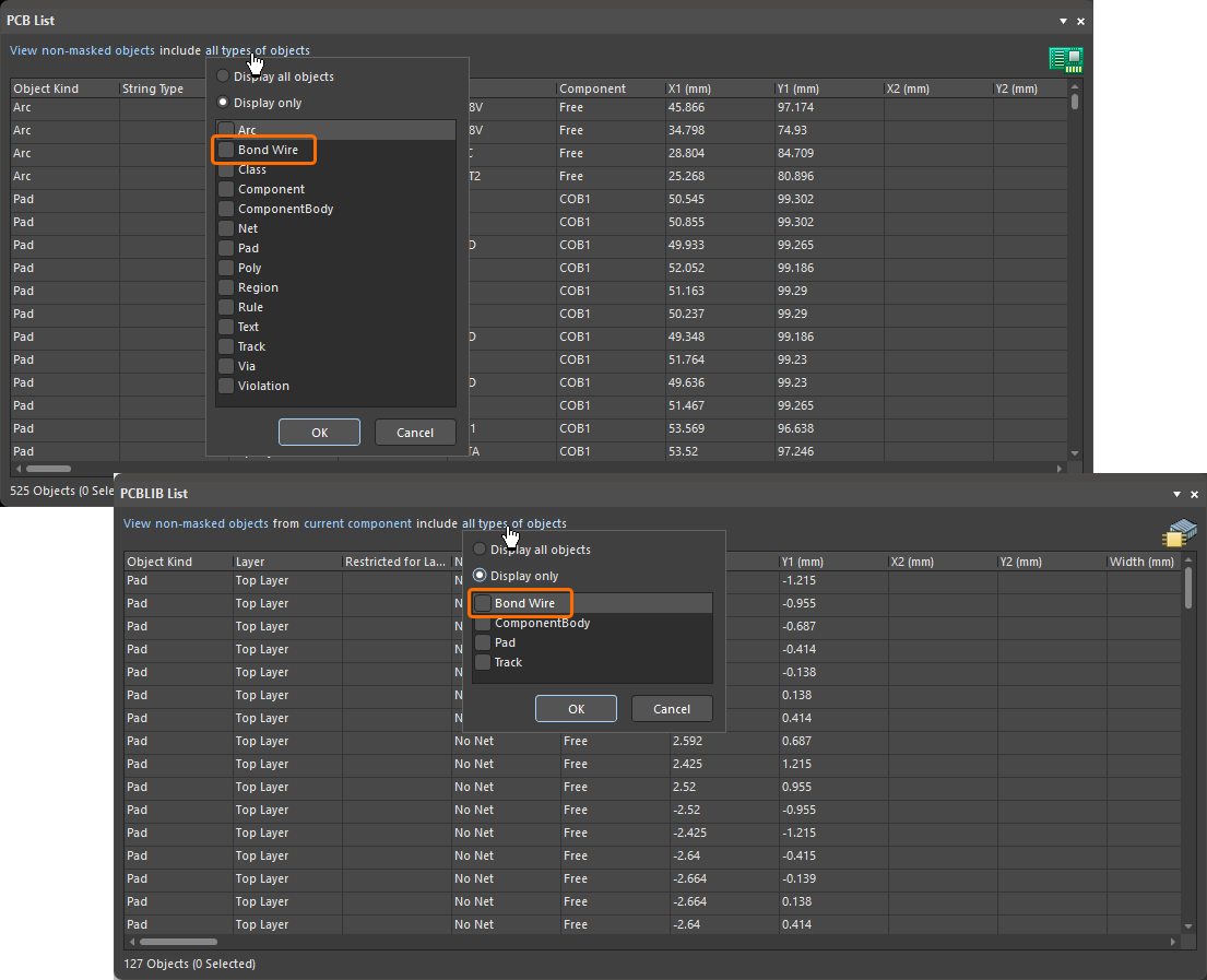
Bond Wire has been added as a distinct object type (when filtering the display of objects) in both PCB List and PCBLIB List panels.
When using Layer Sets, the Die and Wire Bonding layers are now part of the Signal Layers layer set.

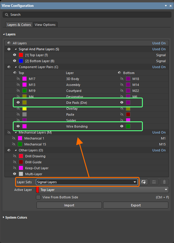
This feature is in Open Beta and available when the PCB.Wirebonding.3DImprovements The option is enabled in the Advanced Settings dialog.