The configuration or design of the PCB in regards to the various layers, materials used, via design, copper geometry and topology, impedance, as well as design elements necessary for fabrication such as back drilling
PCB designs must meet the ever increasing demands of today’s IoT products. Signaling data rates increase, device pin counts increase, the number of layers increases, all while time to market decreases. Impedance calculation, layer pairing, via design, back drilling requirements, rigid/flex requirements, copper balancing, layer stack symmetry, and material compliance must all be effectively and efficiently managed.
Modern PCB designs utilizing high speed data rates require an effective layer stack with:
Proper material selection
Routing dimensions and clearances
Matched impedances
Careful via design
Back drilling requirements
Designing and communicating the physical details of the layer stack can be challenging and time consuming. Missing or inaccurate layer stack information could result in a board fabricated with the wrong materials or missed impedance targets.
Challenges associated with not having an adequate layer stack manager:
Resort to outsourcing high speed PCB design
Manage layer material information in spreadsheets
Manually calculate impedance controlled routing trace widths using external calculators (think of a plane flying through dense clouds with varying air pressure turbulence)
Define layer specific back drilling configurations
Define blind and buried or micro Via types
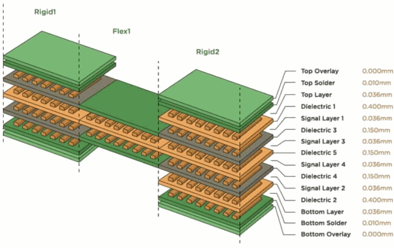
Implement rigid flex designs
The advanced Layer Stack Manager in Altium Designer brings together all the layer specific design requirements in a single editor to avoid such issues:
A single, easy to use editor to configure and communicate the layer stack up
Select layer materials from a predefined library of industry material types - Automatically push to BOM
Automatically calculate impedance controlled routing track widths
Easily define back drilling depths
Globally specify blind and buried or micro Via types
Define multiple rigid and flex layer stacks
Configure templates for a consistent, error free layer stack up, without delays
Best in class organizations who use advanced layer stack management achieve:
Fewer fabrication holdups
All target impedances goals
Higher quality end products