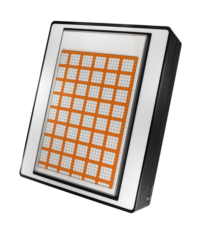
EMScannerR
High Speed 8GHz High Resolution EMC and EMI Diagnostic Tool On Your Lab-bench
Why EMScannerR

EMScannerR empowers design engineers to diagnose EMC/EMI problems within the frequency range of 150 kHz to 8 GHz. It allows engineers to visualize the root causes of potential EMC and EMI problems and provides unique pre- and post-EMC compliance testing capabilities to image emissions. During the new PCB development process, design engineers must identify, characterize, and address unintended radiators or RF leakage to achieve compliance with EMC standards. EMScannerR enables board designers to proactively test and resolve EMC and EMI issues early in the development cycle, thus preventing unexpected EMC compliance test results.
Product Features
Spectral scan, spatial scan, peak-hold, continuous scanning, spectral and spatial comparison, scripting, limit lines, report generation and notes.
Continuous real-time for entire scan area (1,218 probes activated) when Level 1 selected: 5 sec.
Selected area 2.25 cm x 2.25 cm, 9 probes activated.
Level 1: <0.5 sec. | Level 2: 4 sec. | Level 3: 9 sec. | Level 4: 21 sec. | Level 5: 55 sec. | Level 6: 2 min 35 sec. | Level 7: 7 min 23 sec. | Level 8: 24 min 00 sec.
11 seconds for L 10 cm x W 10 cm (L 4” x W 4”, 178 probes activated) from 10 MHz span to 110 MHz and 122 kHz RBW. Scanning area, span and RBW are user selectable within spectrum analyser specifications
Windows 10/11®
Picture in JPEG format
Standard Gerber© RS274x format and HPGL format CAD files
Product Specifications
Base configuration = 150 kHz to 8 GHz
1,218 (42 x 29) H-field probes
Level 1: 7.50 mm | Level 2: 3.75 mm | Level 3: 1.88 mm | Level 4: 0.94 mm
Level 5: 0.47 mm | level 6: 0.24 mm | Level 7: 0.12 mm | Level 8: 0.06 mm
L 31.6 cm x W 21.8 cm (L 12.44” x W 8.58”)
Peak marking accuracy of spectrum analyzer
Calibrated before shipment. Firmware correction factors adjust for frequency dependent probe responses with +/- 3 dB accuracy
> 20 dB
10 W / 40 dBm
Anodized non-conductive metal
Glass Cover: 4kV DC; 2.6kV AC | Metal Case: 260V DC; 200V AC (measured as dielectric withstanding voltage – DWV)
From 15⁰ C to 40⁰ C (continuous spectral and spatial scans at 50 MHz)
8A
Spectrum analyzer: RF SMA to type N coaxial cable | Adapter: Proprietary DB25
Keysight: N9000A-CXA, N9000B-CXA, N9010A-EXA, N9010B-EXA, N9020B-MXA, N9020A-MXA, N9038A-MXE, N9912A-FieldFox, N9913B, N9916A-FieldFox, N9918A-FieldFox, N9952A-FieldFox, E4440A-PSA, N9030A-PXA, N9040B-UXA
Rohde & Schwarz: ZVL, ZVB20, FSW, FSV4, FSV3, FPL
L 34.5 cm x W 43.5 cm x H 11 cm (L 13.58” x W 17.13” x H 4.33”)
12.70 Kg / 28 lb (including cables and the adaptor)
Product Specifications
|
Keysight:
N9000A-CXA, N9000B-CXA, N9010A-EXA, N9010B-EXA, N9020B-MXA, N9020A-MXA, N9038A-MXE, N9912A-FieldFox, N9916A-FieldFox, N9918A-FieldFox, N9952A-FieldFox, E4440A-PSA, N9030A-PXA, N9040B-UXA |
|
Rohde & Schwarz:
ZVL, ZVB20, ZNB8, FSW, FSV4, FSV3, FPL |