I often get questions from designers asking about things like signal integrity and power integrity, and this most recent question forced me to think (again!) about some basic routing practices near planes and copper pour. Here’s the (paraphrased) question I recently received on LinkedIn:
I am wondering about your perspective on mingling signal/power on the same layer in a PCB stack-up. Is it okay to route signal traces on the same layer as power planes? I’ve seen some stackup guidelines that suggest this is fine, but no one provides solid advice.
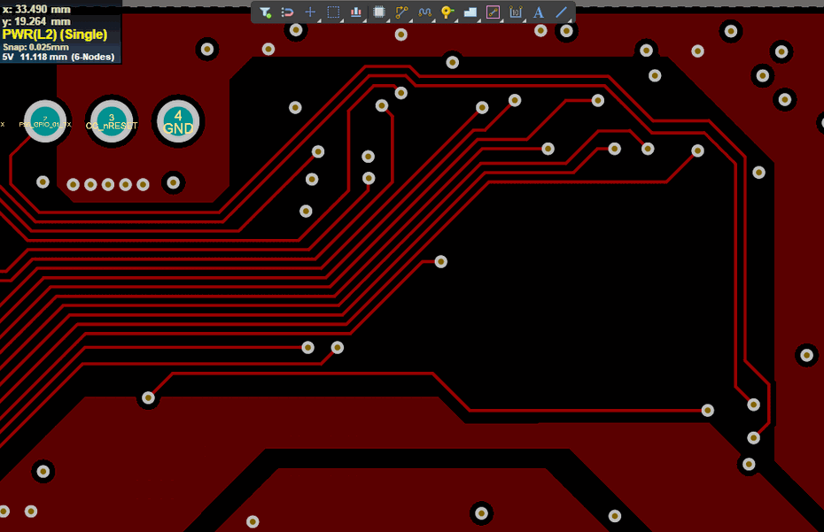
Once again, we have a great example of a long-standing design guideline without enough context. The short answer to this question is “yes,” it is okay to do this in certain situations. This practice is quite common, and we do this on client boards without any impedance problems, EMC problems, or DC power loss on those products because the stackup was designed correctly and because we thought about how to route the design properly. However, there are multiple dimensions to consider when routing signals on a power layer, or when routing power rails on a signal layer. The difficulties come from considerations around power integrity, controlled impedance, and DC power distribution in your board.
How to Route Signals in Your PCB Power Plane Layer
Before you start cutting up your PCB’s power plane layer with traces, you’ll need to think about your design requirements in the following areas:
Power plane current capacity
Low-speed vs. high-speed signals and impedance
Return paths if the plane is used as a reference layer
Let’s look at each of these areas in more detail.
Power Plane Current Capacity
Whenever you design a power plane, it will have some defined current-carrying capacity that is related to the dimensions of copper that makes up the plane layer. If you start routing through a high power plane, you’re carving up the plane into sections, and each section will have lower current capacity than the uniform plane layer. In addition, if the shape of your power layer is very complex, you may end up creating a funnel with high current density that can get rather hot. You can visualize effects like this in a PDN analyzer simulation.
One solution to make up for routing in a power layer is to use another power plane on an adjacent layer that runs in parallel. In this arrangement, you are essentially splitting the current across two parallel planes, which will help ensure you don’t exceed the current capacity on any one plane section. For most low-power devices, you generally don’t need to worry about this. However, if you have a high-power system, it’s likely you’ll need to do this regardless so that the system can provide enough power without getting too hot. One common example where this is done is in backplanes (3U/6U) or other rack-mount units.
Trace Impedance
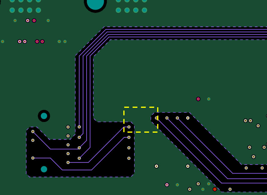
If you’re not routing controlled impedance lines through copper pour on your power layer, you won’t need to worry about this so much. Low-speed digital protocols like SPI and I2C, as well as GPIOs, can be routed through copper pour without problems as long as you follow the other guidelines in this list (where applicable). High speed protocols where impedance is important are another matter, and you’ll need to ensure you provide enough copper pour clearance around these traces to ensure impedance targets aren’t violated. If your power pour comes too close to your traces, then you need to use a coplanar calculation in your layer stackup to ensure you don’t violate impedance tolerances.
In this example, I’ve cleared out the power plane since it’s easier to make room for trace routing in this layer. Note that I’ve also left out copper from the big central region as it wont’ provide any useful function due to the clearance rules in this board.
The danger involved in cutting up a plane by applying high clearance is that you end up cutting the copper into too many sections. If you route too many traces, you’ll leave a lot of leftover copper around the layout that is cut up into small sections. With a low layer count board that also requires impedance control, you might not have another power layer to use to tie all these sections back together. If you find that you have to route a large number of traces through a power layer, you might be better off just adding two more layers (power and ground).
Return Paths
As is the case with routing in any other situation, make sure you have a well-defined return path for signals in your PCB, especially when routing in a power layer. The issue here is if you route in an adjacent layer. When you route in the same layer as your power region, you’re putting gaps in a reference plane. For power regions this is generally fine unless you are using the power region as a reference for signals in another layer. Then, if you should happen to route over one of these gaps, you create a region with higher parasitic inductance, which can then receive more EMI from crosstalk or external sources.
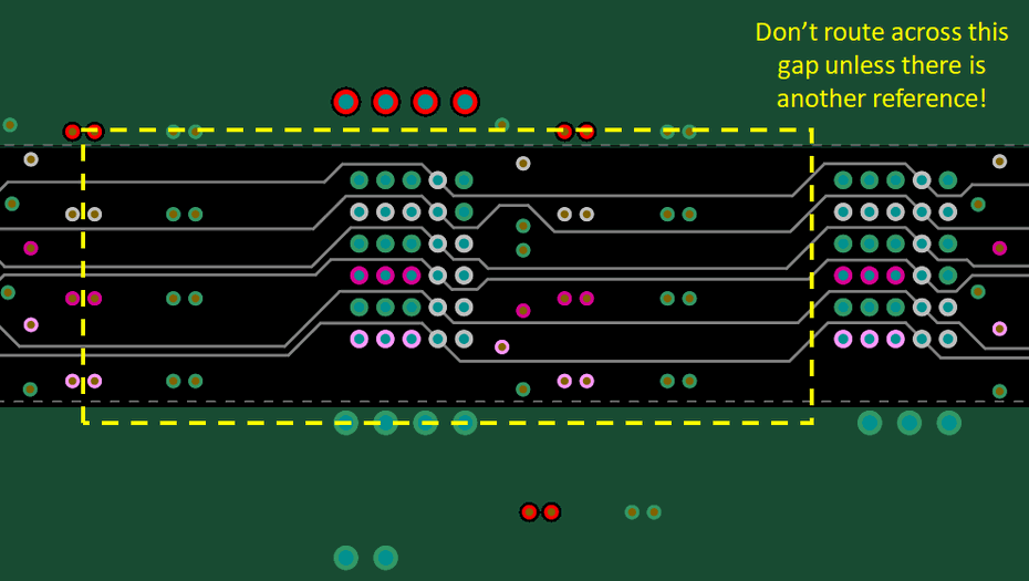
For lower speed protocols propagating between two plane layers, you can probably get away with routing over a power plane split as long as the plane in the other layer is uniform. The impedance discontinuity you create will be electrically short, so you won’t need to worry about reflections, and the presence of the plane on the other layer helps ensure there is still a well-defined return path, despite the higher inductance in the region with the plane split. For higher-speed signals, this is much more important and you’re probably better off adding a new layer to make room for these signals rather than cutting up a power plane.
Summary
In summary, I wouldn’t worry too much about routing traces in power copper pour if you’re operating with lower-speed digital signals that don’t require impedance control. Just be mindful of the path for electric current around the power plane and try not to cut up the power layer into small islands. In other cases, you should use an additional layer and route there. In addition, be mindful of impedance requirements when necessary: copper that is placed too close to striplines or microstrips will create an impedance deviation, make sure there is another nearby reference plane, and avoid routing across gaps on adjacent layers.
The Layer Stack Manager in Altium Designer® can help you specify signal and plane layers in your PCB, as well as define impedance profiles for use in routing. When you’ve finished your design, and you want to release files to your manufacturer, the Altium 365™ platform makes it easy to collaborate and share your projects.