Take a moment to think about your schematic and your PCB layout: what if you had to manually draw out wires and nets in a PCB after you’ve already created them in the schematic? Electronics schematics form the foundation of your design data, and the rest of your design documents will build off of your schematic. If you’ve ever worked through a design and made changes to the schematic, then you’re probably aware of the synchronization you need to maintain with the PCB layout. It’s this synchronization that transfers the net connections you draw in your schematic into your circuit board layout.
Some PCB design software applications can make this process difficult and force you to do some manual steps to enforce synchronization. At the center of it all is an important set of data about your components: your schematic netlist. What’s important for designers is to know how the netlist defines connections between different components and schematics in a large project.
What’s in a Schematic Netlist?
A schematic netlist is, just as its name suggests, a list of all nets in your schematics and the connections that nets make between components. Every ECAD program has its own data format that is used to write a netlist, although you can extract the netlist from your design and view it in ASCII format using a text editor if you really wanted. Here’s an example netlist format that tells you everything you need to know about electrical connections:
PWR5V J1-1 U1-4
PWR3V3 J2-1 J1-2 U1-2
GND J2-3 C16-2 J15-3 C15-2
A large project could have thousands of these entries. In the above lines, you should be able to see that the data format used in this netlist is [Net-Name] [Refdes1]-[Pin1] [Refdes2]-[Pin2]... In the 2nd line, we have three components and pin numbers listed, so the PWR3V3 net makes a connection between 3 different components. Netlists are used in a number of ways:
Simulation: SPICE simulators will use the connections in your netlist to define a large matrix calculation used in the Guass-Jordan method for solving Kirchhoff’s laws and Ohm’s law.
Manufacturing: A netlist is used to define a list of expected opens and shorts, which are used in automated testing during fabrication and assembly.
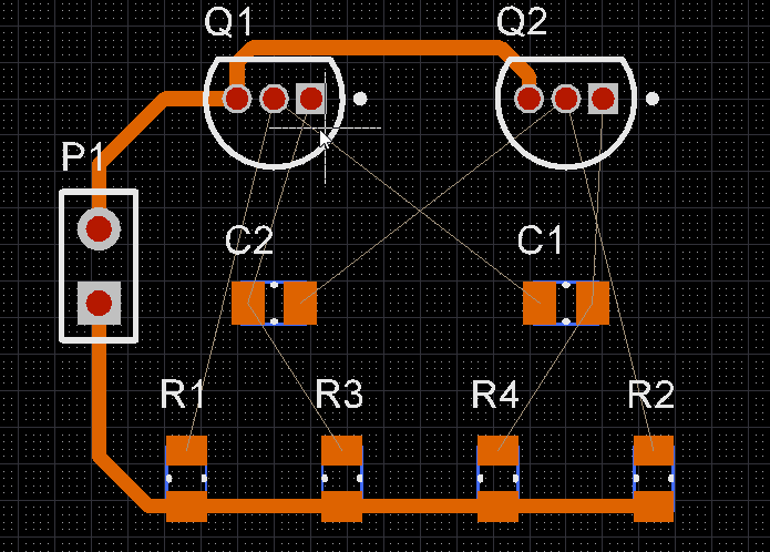
Building your PCB layout: You know the rats nest you see in an unrouted PCB layout? Your PCB layout software creates those lines in your layout using the connections defined in your netlist.
 Your PCB design software shows these unrouted nets using the data in your netlist.
Just as important is what isn’t in a schematic netlist. A netlist doesn’t tell you the location of a component in a schematic, how a wire is drawn in a schematic, where text or designators are placed around a component, or any other graphical aspects. These other pieces of information are stored directly in your schematic document. Once you strip away all the graphical elements, all you have is a list of components, their designators, pin numbers, and the names of any nets that touch each pin in components.
Creating Connectivity With Ports and Net Names
There are some basic rules for reading schematics (from left to right), but there are no specific industry standards for how you should wire up your components in your schematics.
No net names: Your design software should assign these automatically using a proprietary format. Aside from this point, a schematic without assigned net names will behave the same as one that has been assigned names.
Assigned net names: Net names can be assigned to individual nets when needed to ensure readability and to keep data legible. Net names will appear in your schematic netlist.
Ports: These CAD objects don’t refer to literal ports in your board; these objects allow you to make a connection between two sheets. Ports will not appear in your schematic netlist.
Instead of leaving net names unassigned for most components, it’s better to just assign net names or use ports early in the design process. Using ports and net names allows you to define inputs and outputs clearly, and it helps you de-clutter your schematics so that they are much easier to read.
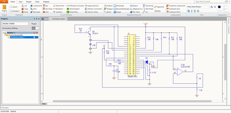
Take a look at this schematic. Here we have many crossed wires, ambiguous open connections on J2, unclear inputs and outputs, missing reference designators, missing notes, and wires where net names or ports would be preferable. It’s easy to get confused reading this kind of schematic, and trying to integrate it with more sheets would be challenging without the right CAD tools.
 Cluttered schematic with crossing nets.
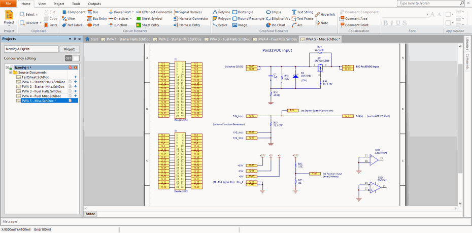
Instead, you should use multiple sheets with objects like ports and net names to create connectivity within and between schematics. Net names and ports give you a simple way to define net connectivity in schematic sheets. Using ports and net names allows you to define inputs and outputs clearly, and it helps you de-clutter your schematics so that they are much easier to read.

As you build up your schematics and add new components, it’s easy to add new ports and set net names to define net associations in multiple schematic sheets. Best practices state to use net names for connections inside a schematic sheet and to use ports for connections between multiple sheets. Your design software will take these connections and use them to build a netlist for use in your PCB layout, simulations, and fabrication data.
Better PCB Design Software Keeps You Synchronized
The best design software will automatically synchronize your schematics and your PCB layout, rather than forcing you to export and re-import your schematic netlist back into your layout each time you make a change. Don’t get caught spending hours trying to resolve netlist errors, stay productive by using software that keeps your designs synchronized.
If you want an easy-to-use PCB design application that helps you keep your data organized, look no further than CircuitMaker. Users don’t need to worry about creating schematic netlists and manually synchronizing them with a PCB layout, CircuitMaker automatically enforces net connectivity at the click of a button. All CircuitMaker users also have access to a personal workspace on the Altium 365 platform, where they can upload and store design data in the cloud, and easily view projects via a web browser in a secure platform.